Illustrated Semiconductor Manufacturing Process
Overview of Semiconductor Manufacturing
01

Wafer Manufacturing

Wafer manufacturing involves growing a single-crystal ingot from high-purity silicon and producing a flat,
high-precision substrate for semiconductor circuit formation through slicing, polishing, and cleaning.
Single Crystal Growth
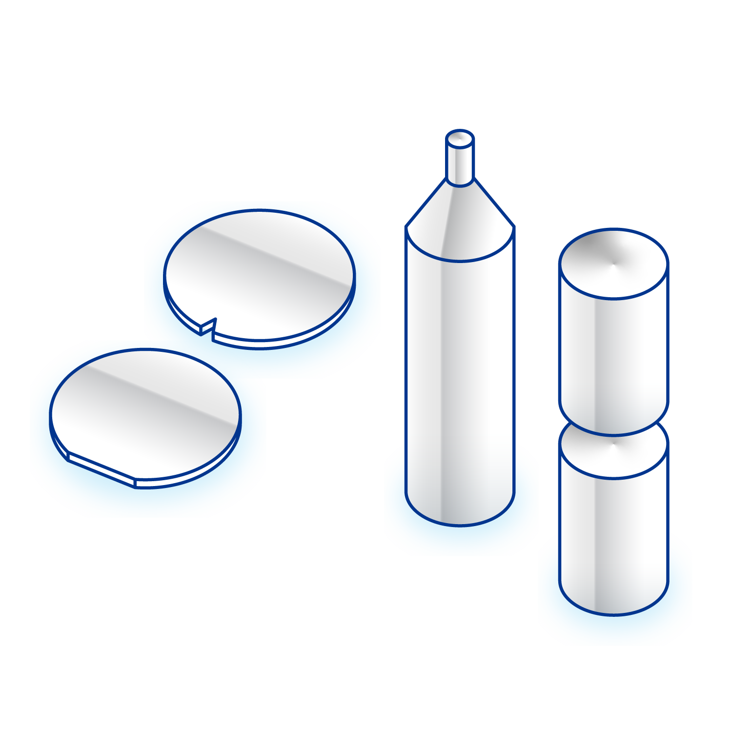
Silicon raw material is melted at high temperature, a seed crystal is brought into contact, and by slowly pulling it upward while rotating, a cylindrical single-crystal ingot is formed.
Diagram of the lifting process
Slicing
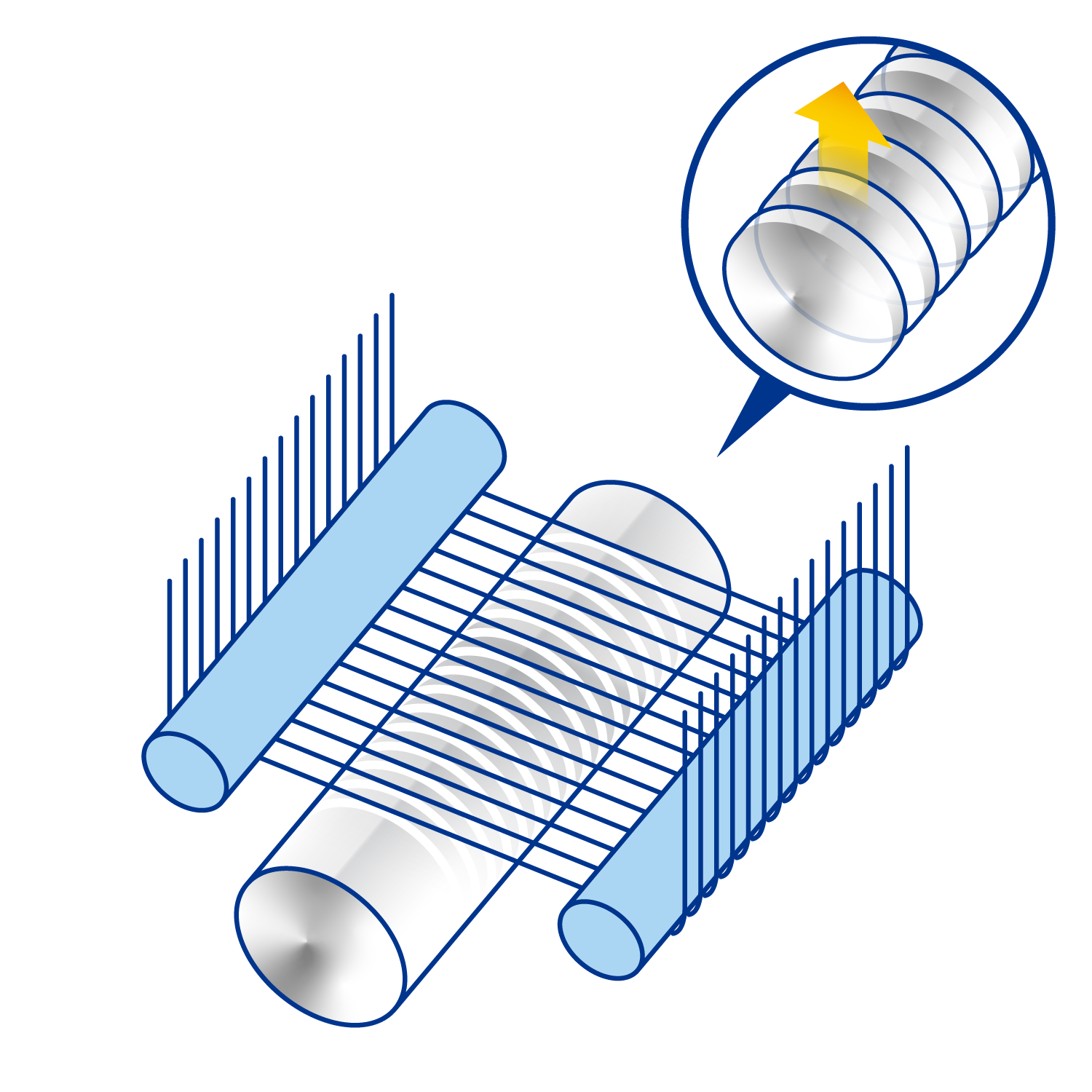
The high-purity silicon single-crystal ingot is sliced using a wire saw or similar equipment and cut into a uniform thickness. The sliced ingot is separated into wafers, cleaned, and then stored in cassettes.
Diagram of the cutting and cleaning process
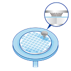
Bevel Processing (Edge Chamfering)
After slicing, the wafer edge is polished to form the desired shape and smooth the shape.
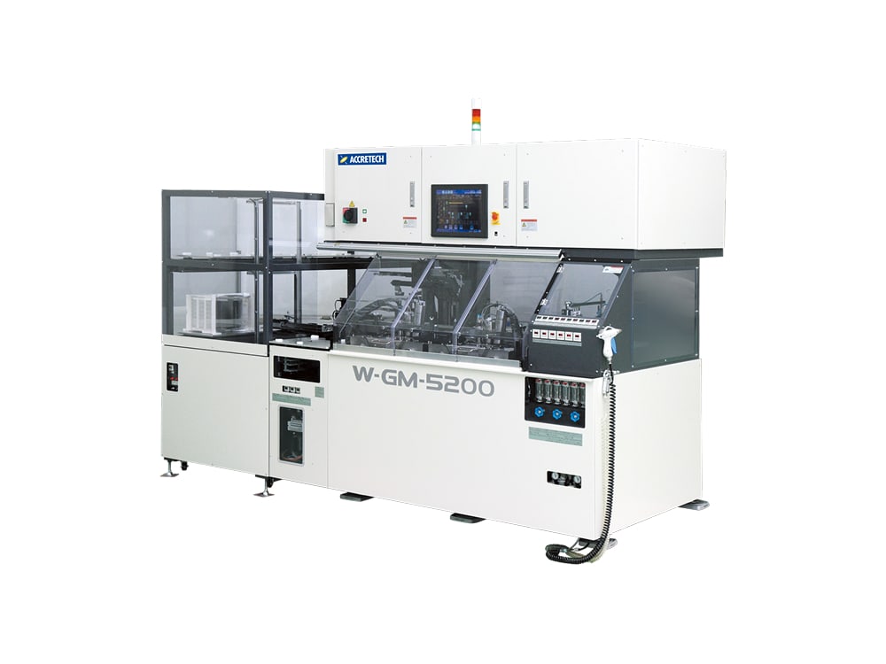
Edge Grinding Machine
In semiconductor manufacturing, improving edge quality has become an essential process. We provide various proposals to meet customer requirements.
Edge Grinding Machine
View product details
Edge Grinding Machine
View product details
Diagram of the edge grinding process
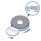
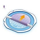
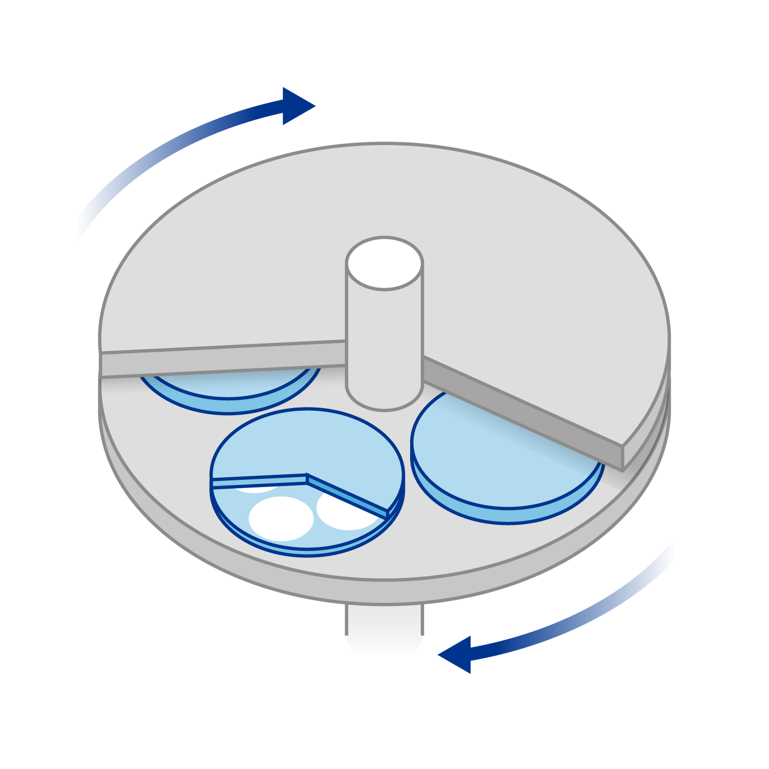
Lapping
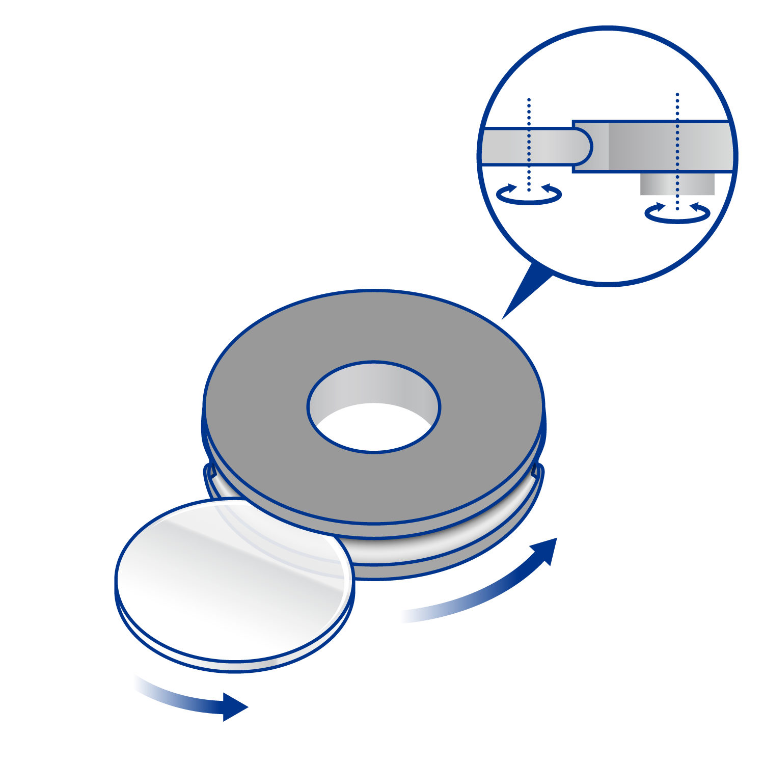
Both sides of the wafer are planarized using a polishing plate and abrasive to achieve a uniform thickness.
Diagram of the wrapping and polishing process
Etching
Damage caused by mechanical processing such as slicing and lapping is removed using chemical solutions.
Diagram of the wrapping and polishing process
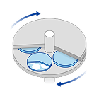
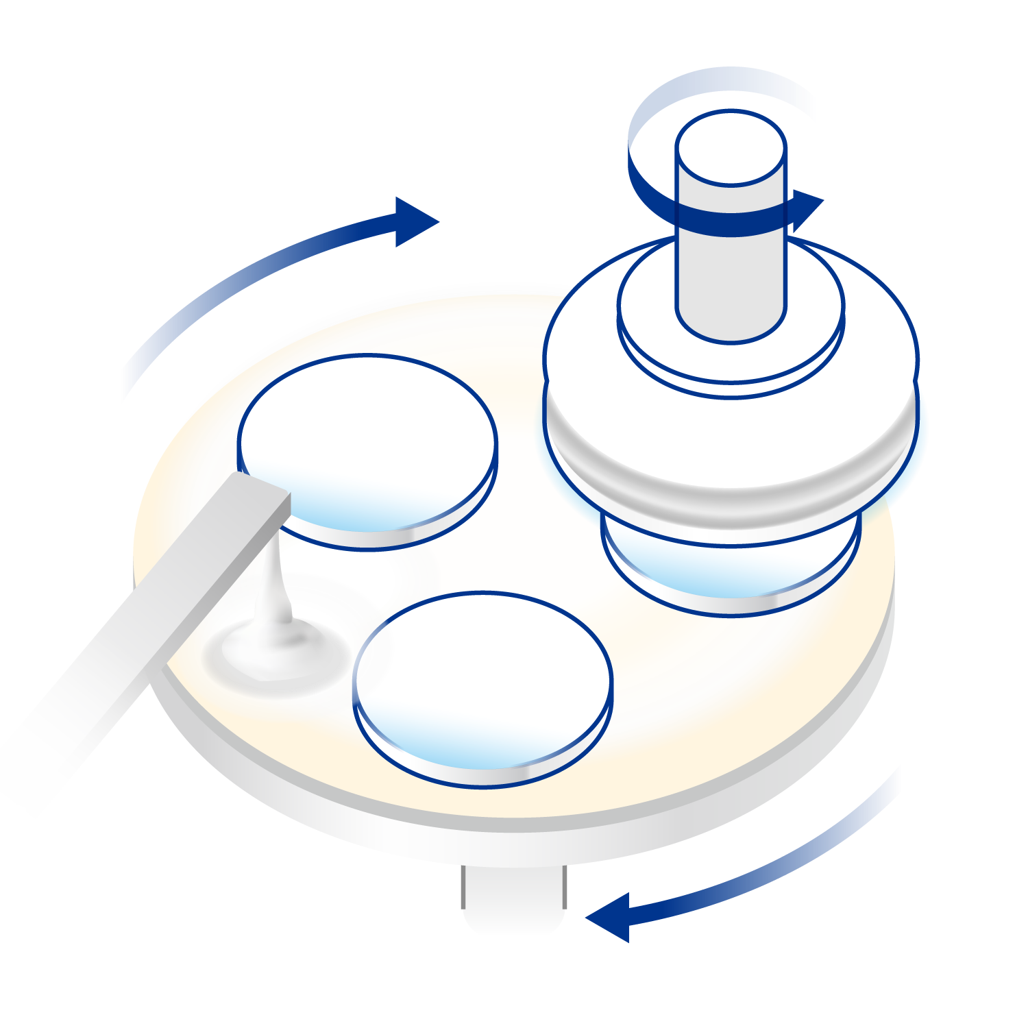
Polishing
Using a chemical solution containing fine abrasive grains and a polishing pad, minute wafer surface irregularities are removed and further planarization is achieved.
Diagram of the polishing process
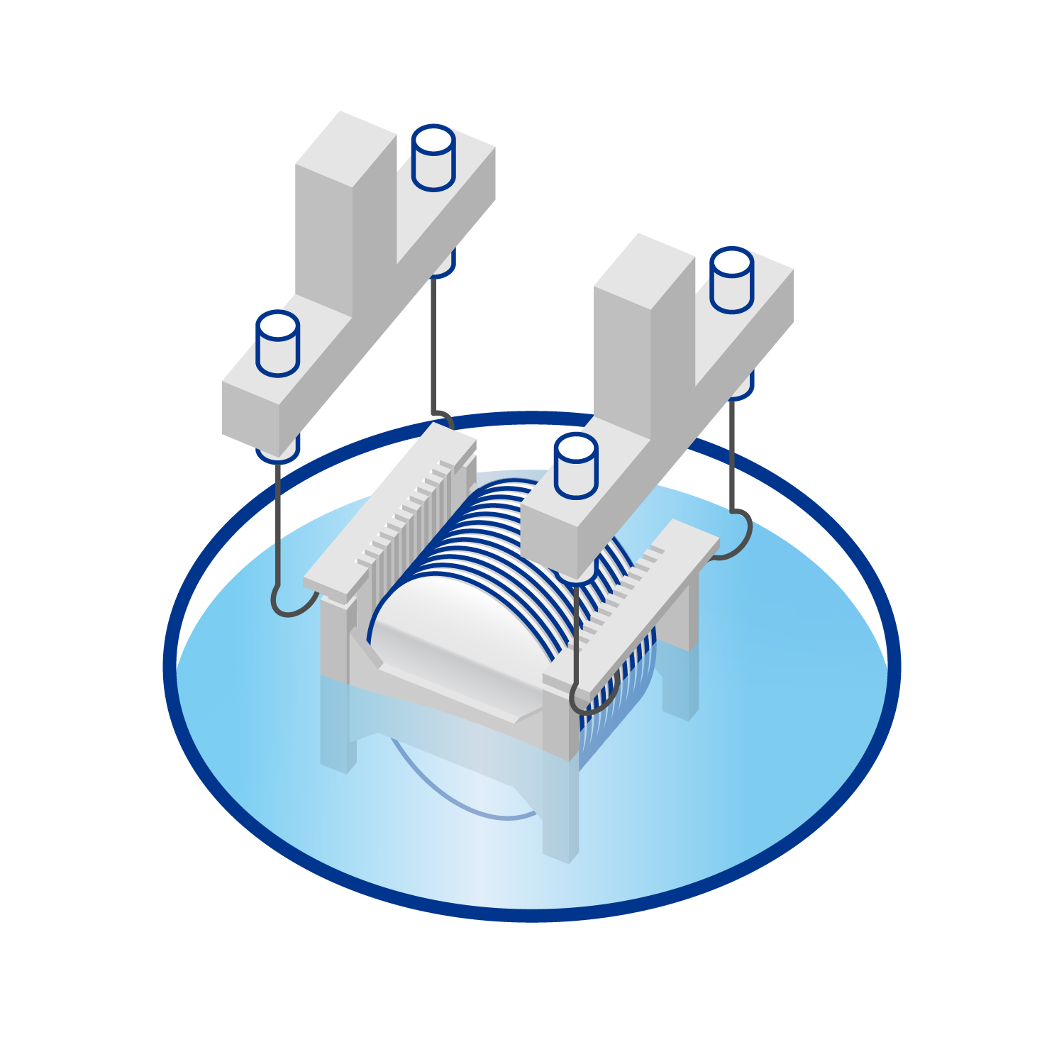
Cleaning
Residual substances and contaminants on the wafer surface are removed using ultrapure water and chemical solutions. The wafer is then rinsed with ultrapure water and dried to maintain a clean, high-quality surface.
Diagram of the cleaning process
02

Front-End

Front-end involves constructing semiconductor circuits on a silicon wafer by repeatedly performing oxidation,
photolithography, etching,thin-film formation, ion implantation, and other processes using microfabrication technology.
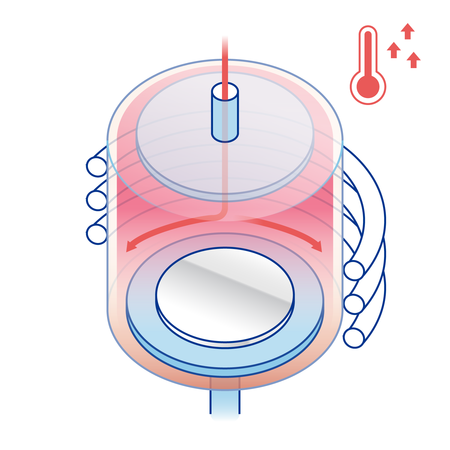
Oxidation
The wafer is processed in a high-temperature oxygen or steam environment to form a silicon oxide film on the surface. This oxide film functions as an insulating layer and improves the electrical characteristics of transistors and other devices.
Diagram of the oxidation process
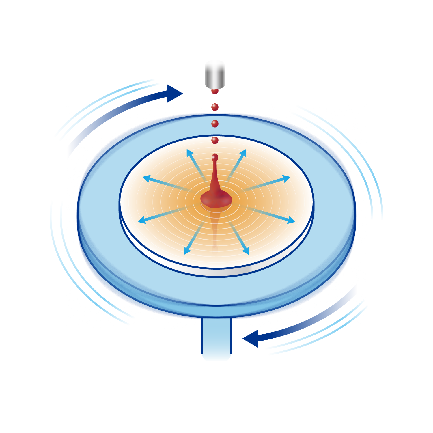
Resist Coating
A photosensitive resin (photoresist) is applied uniformly to the wafer surface. This forms the basis for accurately creating circuit patterns in the subsequent exposure process.
Diagram of the diffusion process
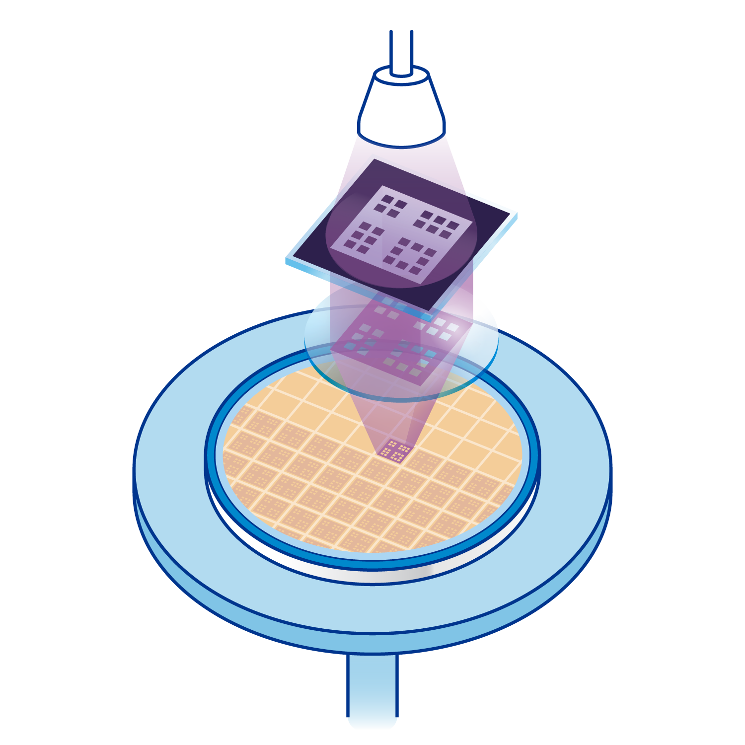
Exposure and Development
Ultraviolet light or an electron beam is applied to the resist-coated wafer through a mask (on which the circuit pattern is drawn). The exposed resist is then removed using a developer, revealing the circuit pattern on the wafer.
Diagram of the lithography process
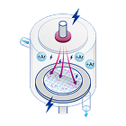
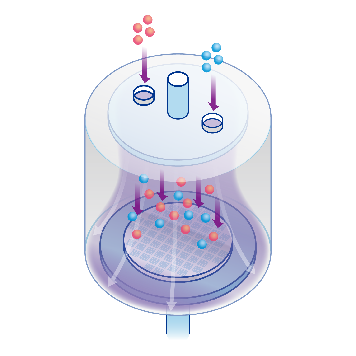
Etching
Areas not protected by the resist are removed by etching to form the circuit pattern.
Diagram of the etching process
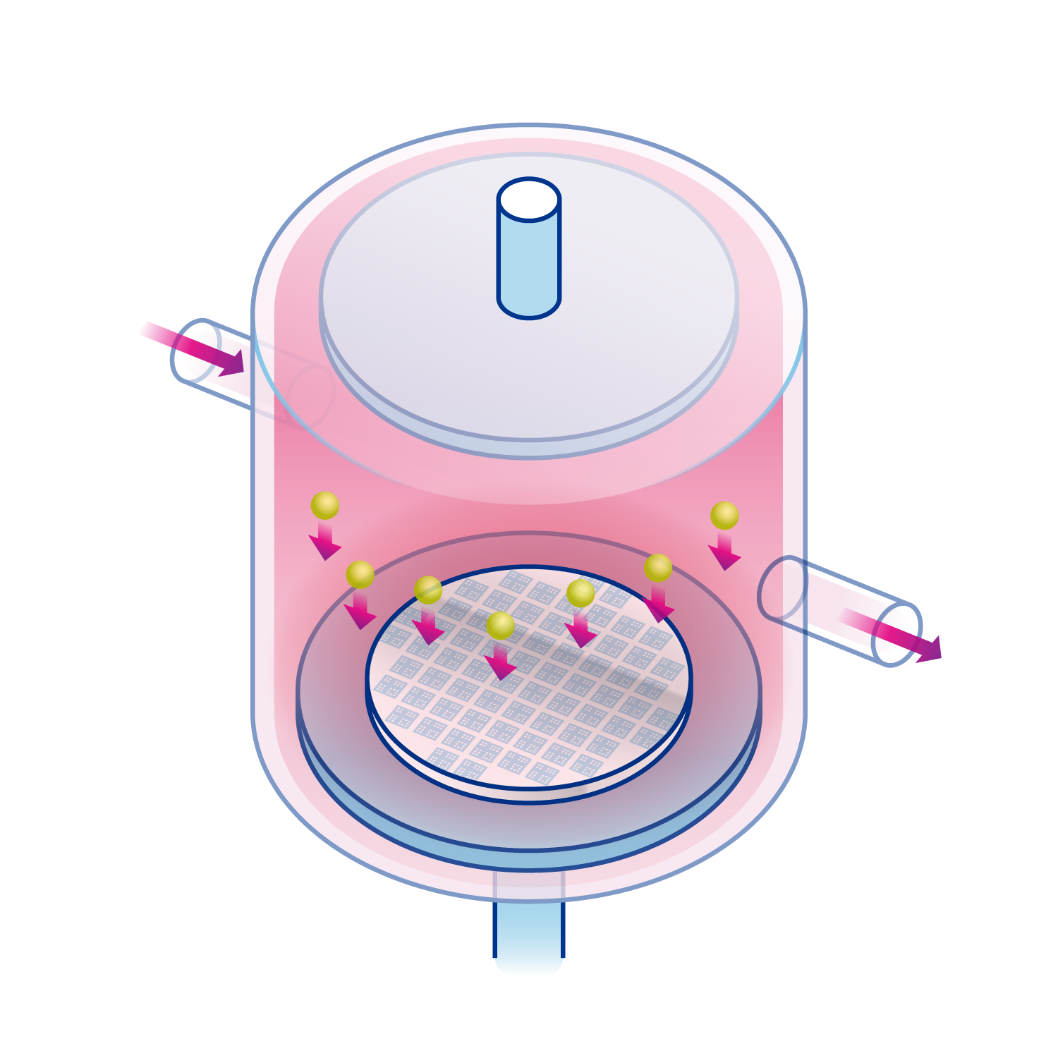
Ion Implantation
To embed specific impurities (dopants) into the wafer with high precision, ionized dopants are accelerated and implanted by colliding them with the wafer surface. This controls electrical characteristics and forms device functions such as transistors.
Diagram of the film deposition process
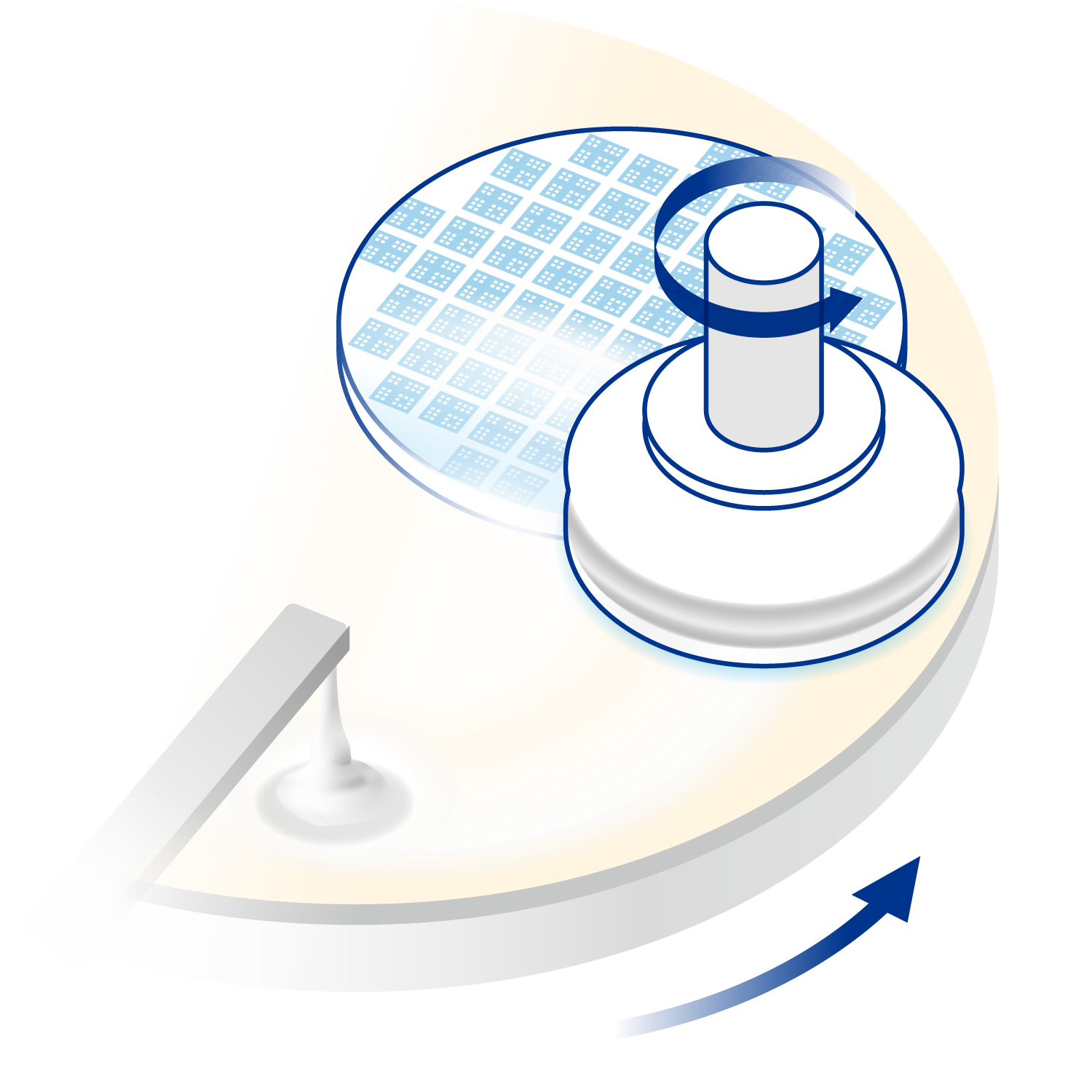
Planarization (CMP)
Using a polishing pad and slurry (chemical solution containing abrasive), the wafer surface is polished through a combination of mechanical processing and chemical reactions. This process planarizes surface irregularities generated during multilayer formation.
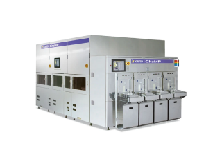
Chemical Mechanical Planarizer
By integrating the technologies of precision measuring instruments and semiconductor manufacturing equipment that we have cultivated thus far, we propose chemical mechanical planarizers (ChaMP series) compatible with various sizes that fully meet the process performance required for advanced devices, as well as the demands of mass production factories.
Chemical Mechanical Planarizer
View product details
Chemical Mechanical Planarizer
View product details
Diagram of the planarization process
Repeat this procedure
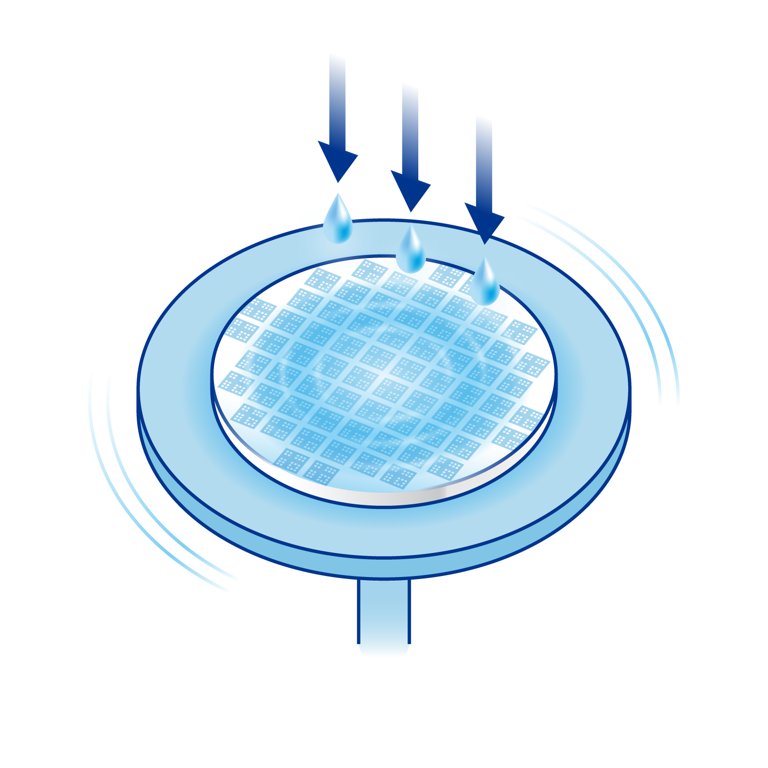
Cleaning
Ultrapure water and chemical solutions are used to remove fine particles, organic substances, and metal contamination adhering to the wafer surface.
Diagram of the cleaning process
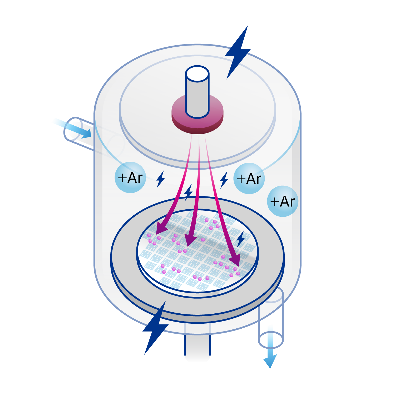
Electrode Formation
After forming an insulating film, openings are created by etching the pattern formed through exposure and development, and metal is filled in by sputtering or vapor deposition.
Diagram of the electrode formation process
03

Wafer Test

Wafer test involves electrically inspecting each chip on the wafer formed during the front-end to distinguish between good and defective products.
Measurement is performed using a probing machine, and defective products are managed by marking or data.
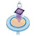
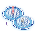
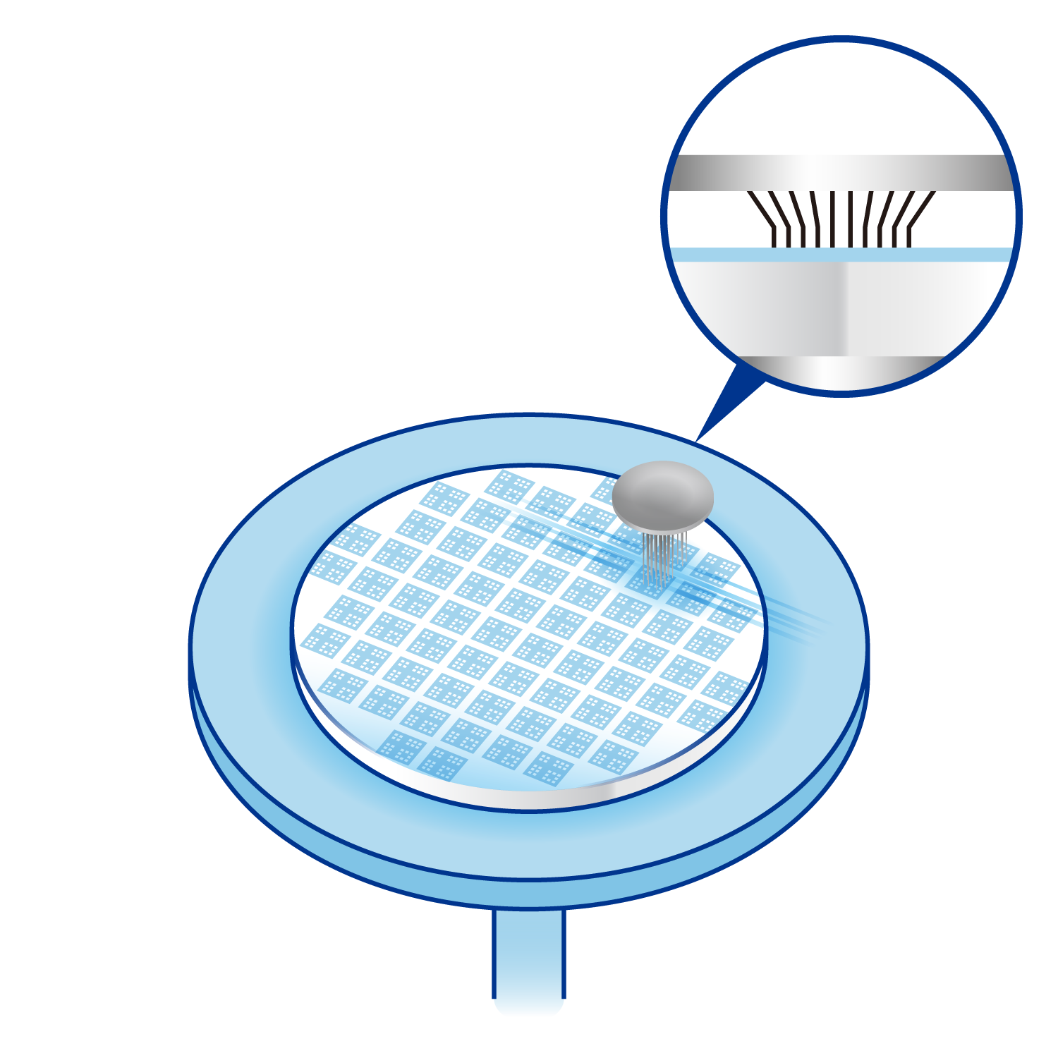
Wafer Probing
Needle-like electrodes called probes are brought into contact with the circuit to evaluate electrical characteristics. This is generally also referred to as wafer inspection.
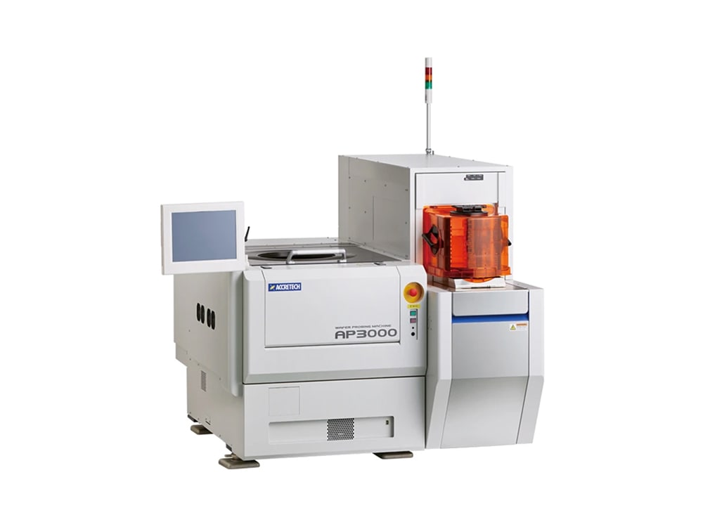
Probing Machine
This is a wafer transport and positioning machine that accurately brings probes into contact with all IC chips formed on the wafer and tests their electrical characteristics by applying current. Tokyo Seimitsu develops new machines tailored to the features of new devices and provides them along with technology to customers worldwide.
Probing Machine
Probing Machine
View product details
Probing Machine
Probing Machine
View product details
Diagram of the wafer testing process
04

Back-End

Back-end involves separating good chips from the wafer, packaging them, and completing them as products.
The wafer undergoes dicing, die bonding, wire bonding, molding, and final inspection before shipment.
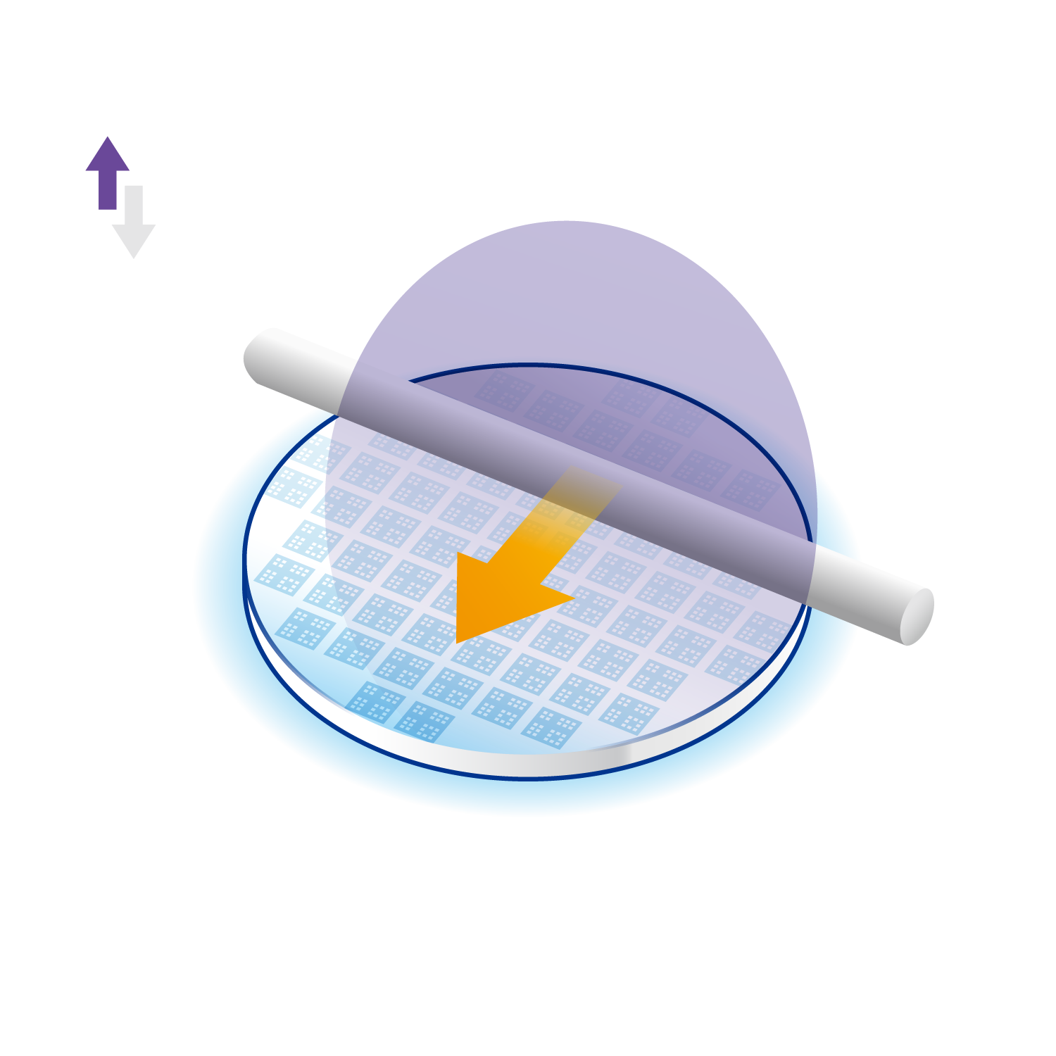
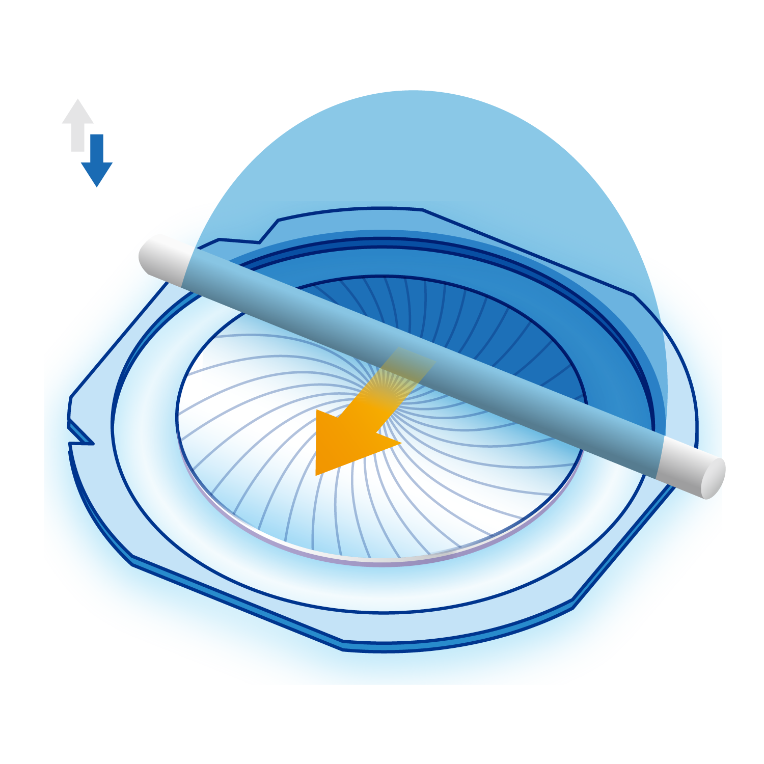
Surface Protective Tape Application
A protective tape is applied to the device side of the wafer to protect the surface from physical damage and contamination during back surface grinding.
Diagram of the grinding process
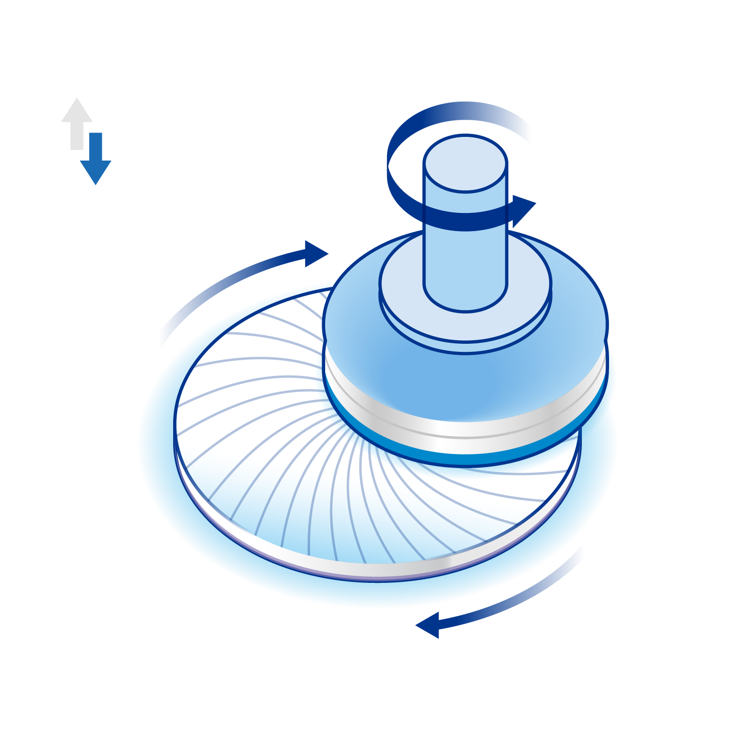
Back Surface Grinding
A grinding wheel containing diamond abrasive grains is rotated at high speed to grind the wafer down to a specified thickness, making it thinner. This process contributes to device miniaturization and improved thermal characteristics. In recent years, demand for ultra-thin processing below 10 microns has increased.
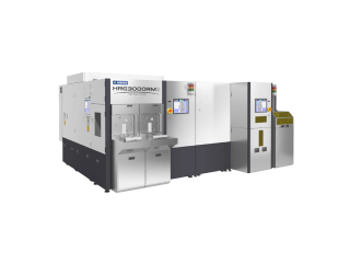
High Rigid Grinder
This is a machine that performs planar processing of wafers using a grinding wheel. It is equipped with our proprietary high-rigidity mechanism, achieving high precision, high throughput, and low-damage processing.
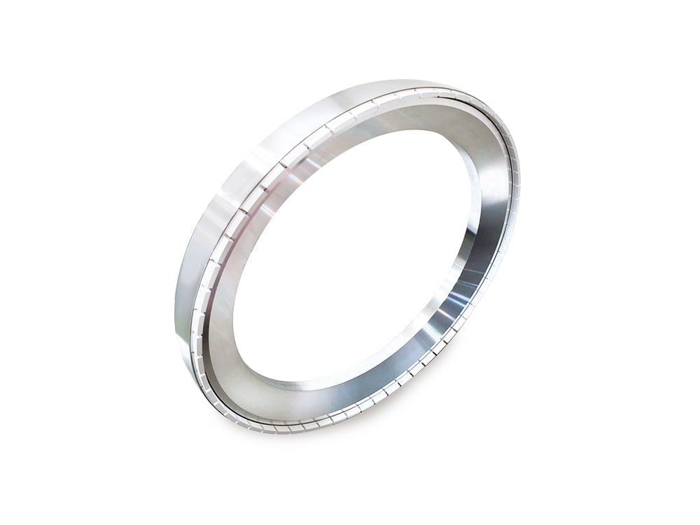
Grinding Wheel
The grinding wheel is specially tuned for use with the high rigid grinder. It maximizes the performance of the high rigid grinder and achieves low wear, low damage, and mirror-finish processing. It is used in combination with the high rigid grinder.
High Rigid Grinder
High Rigid Grinder
View product details
Grinding Wheel
Grinding Wheel
View product details
High Rigid Grinder
High Rigid Grinder
View product details
Grinding Wheel
Grinding Wheel
View product details
Diagram of the back surface grinding process
Dicing Tape Mounting
The thinned wafer is attached to a ring frame with dicing tape and securely fixed in place. This prevents damage to the thinned wafer and ensures chip retention during dicing.
Diagram of the dicing tape mounting process
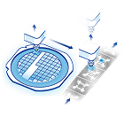
Surface Protective Tape Removal
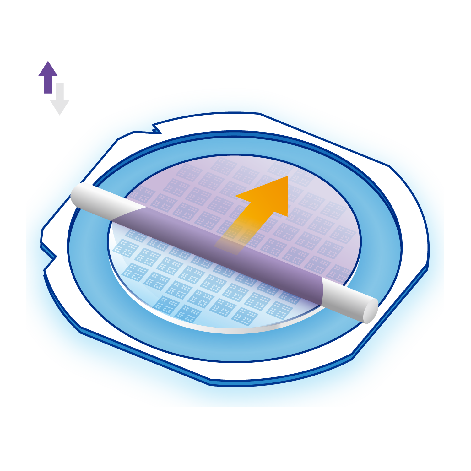
The protective tape applied to the device surface of the wafer is carefully removed.
Diagram of the surface protection tape removal process.
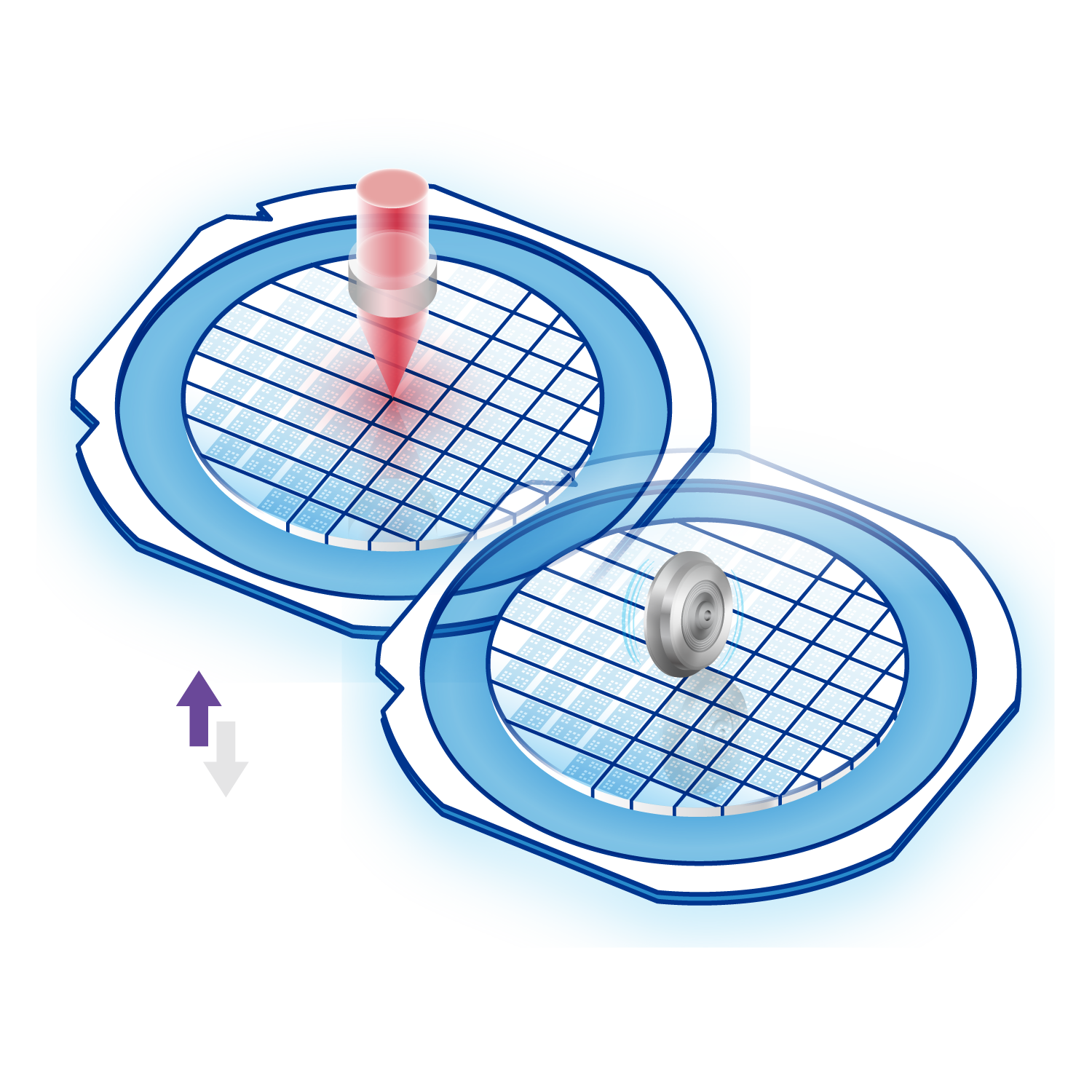
Dicing
This cuts the wafer into individual chips (dies). Generally, cutting is performed by rotating a diamond blade at high speed. In recent years, laser-based dry processes have also increased and are used according to requirements.
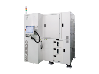
Dicing Machine
This machine separates a wafer on which multiple ICs are formed into individual chips through a cutting process. In response to the diversification of dicing processes driven by the advancement of various devices, we provide high-throughput and high-quality processing by combining our long-established "high-precision positioning technology" with optimal processing methods (blade dicing and laser dicing).
Precision ACCRETECH Blades
Tokyo Seimitsu’s precision ACCRETECH blades combine innovative development technology with application technology, offering a product lineup that supports all types of workpieces and processing applications, meeting the demand for "high quality and low cost" required by the times.
Dicing Machine
Dicing Machine
View product details
Precision ACCRETECH Blades
View product details
Dicing Machine
Dicing Machine
View product details
Precision ACCRETECH Blades
View product details
Diagram of the dicing process
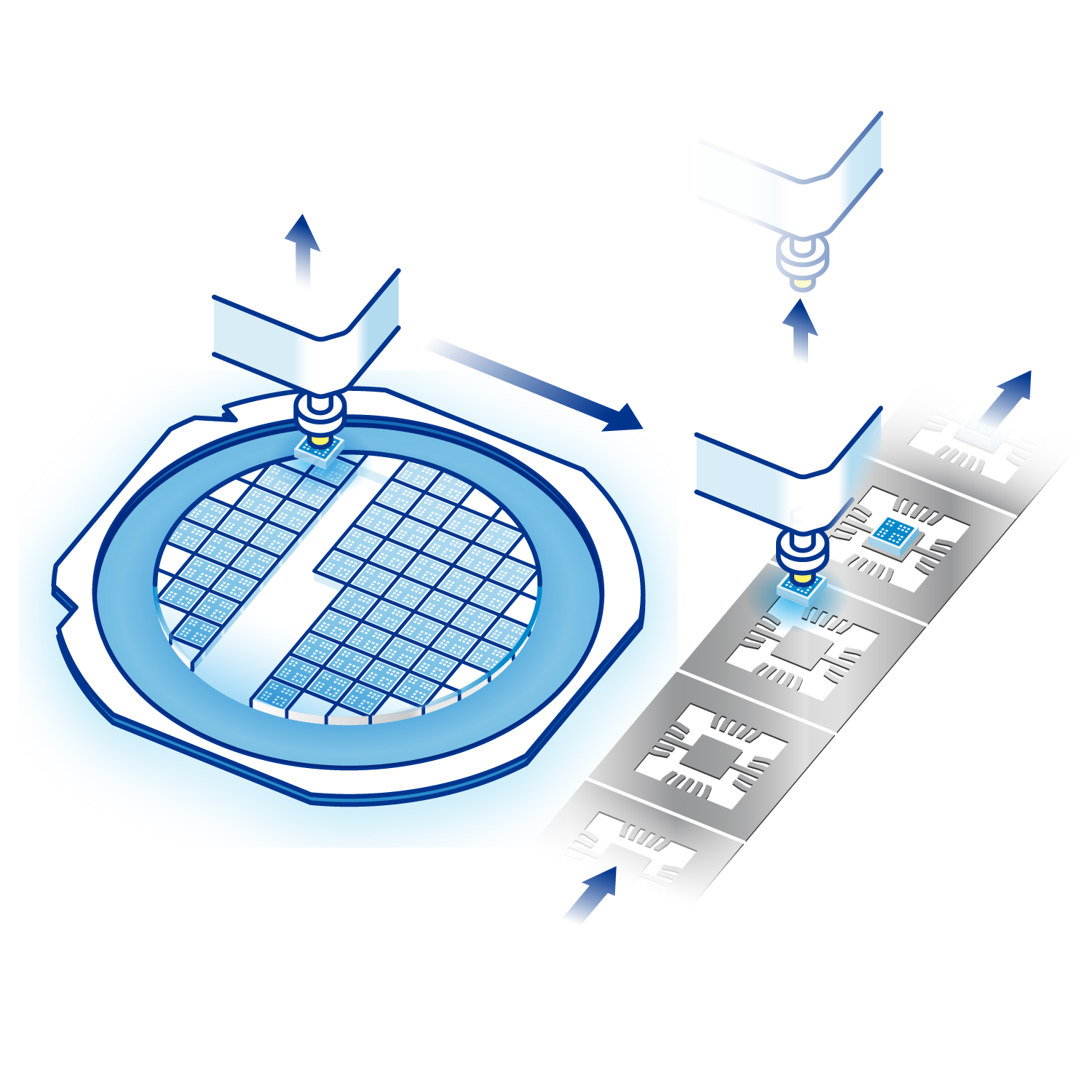
Die Bonding (Mounting)
This bonds individual chips (dies) to a package substrate. The separated chips are placed at precise positions on the substrate using a die bonder and then cured to secure adhesion.
Diagram of the bonding process
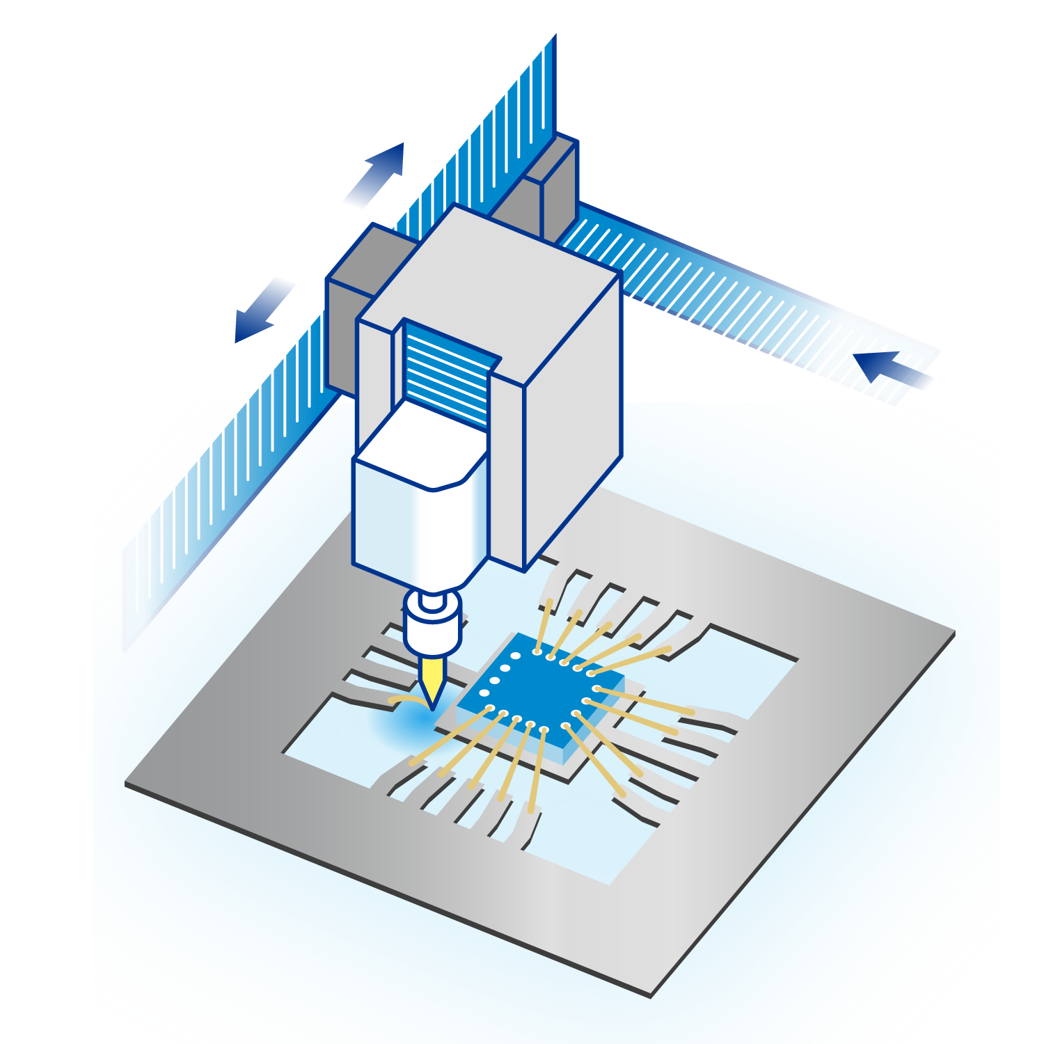
Wire Bonding
This electrically connects individual chips (dies) to a package substrate or lead frame. The pads of the chip fixed to the substrate and the substrate terminals are connected using fine gold or aluminum wires with a wire bonder by applying ultrasonic sound, heat, and pressure.
Diagram of the wire bonding process
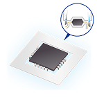
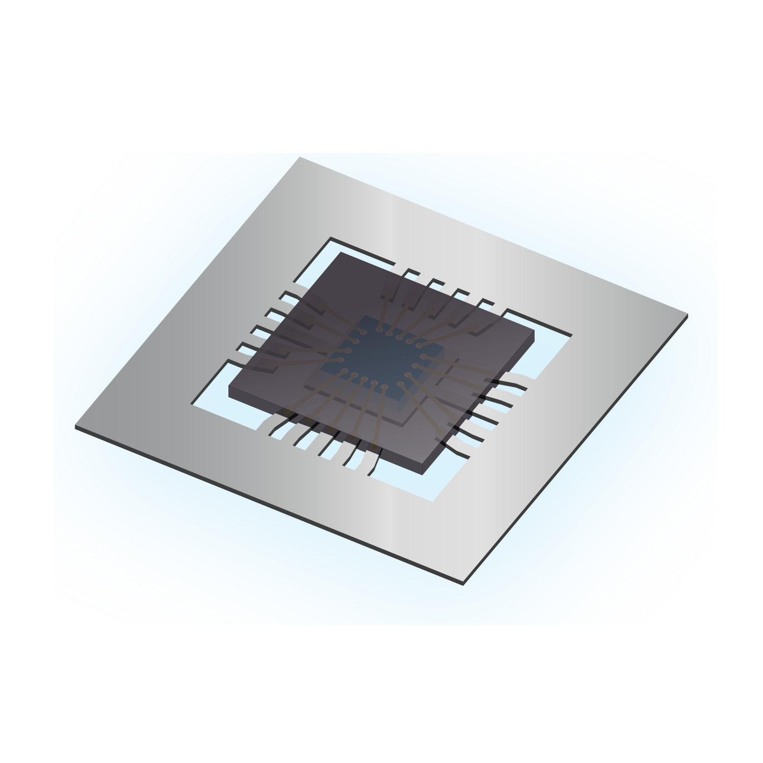
Molding
The chip and substrate after wire bonding are encapsulated with a sealing material such as epoxy resin to protect them from physical damage and environmental factors.
Diagram of the molding process
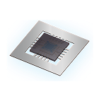
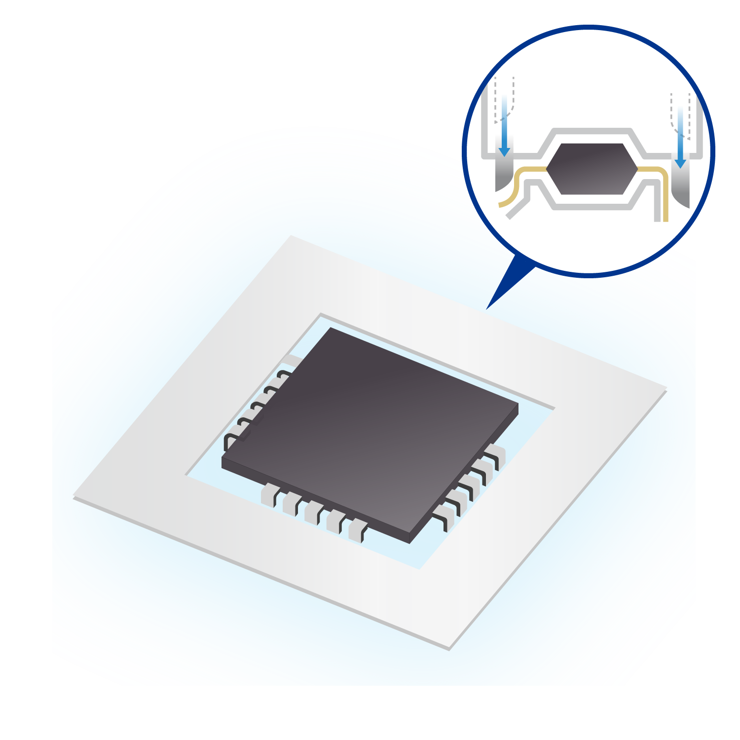
Trim and Form
Unnecessary portions of the lead frame that are attached to the packaged device are cut off, and the packaged device is shaped into a form that allows accurate mounting on a printed circuit board.
Diagram of the trimming and forming process
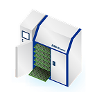
Burn-In(Temperature and Voltage Test)
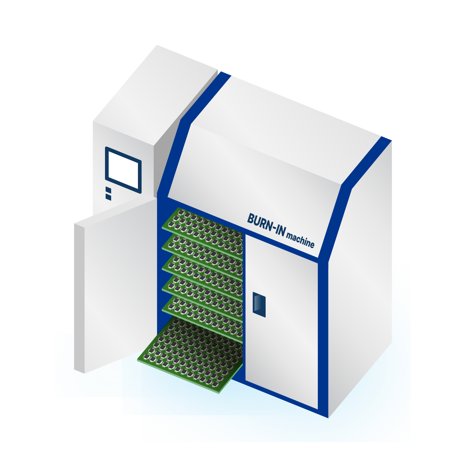
Multiple packaged devices are set on a dedicated board and operated for several hours to several days in a burn-in chamber under high temperature (typically around 125°C) and electrical stress (rated voltage and current). This simulates operation under harsh conditions and enables early detection of initial failures.
Diagram of the burn-in (temperature and voltage test) process
Inspection
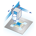
Appearance inspection is performed using a high-resolution inspection system to check for physical defects such as cracks and foreign matter adhesion.
Diagram of the final testing process
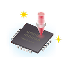
Marking
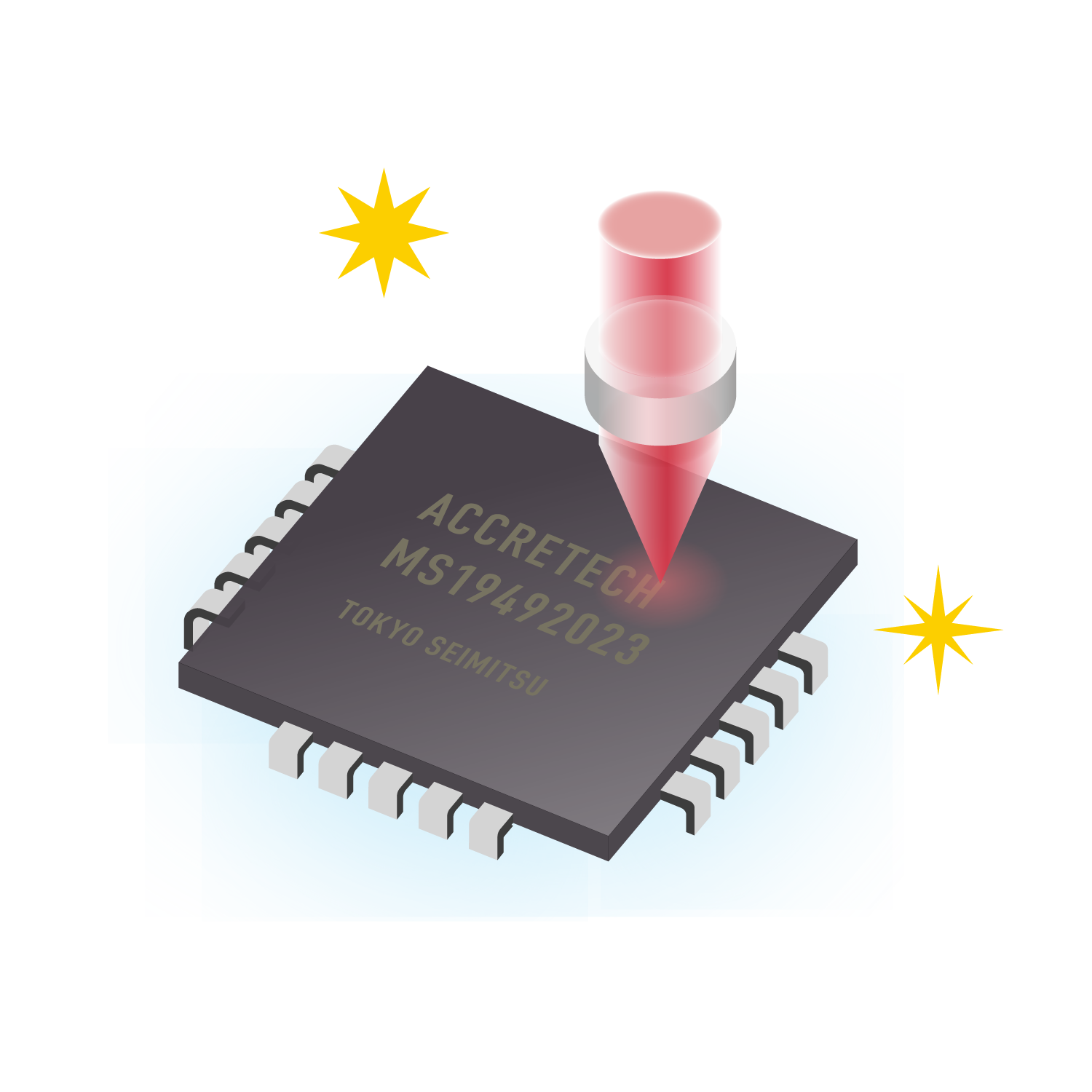
Identification information is engraved on the completed semiconductor devices. Marking is performed to facilitate product traceability and identification.
Diagram of the marking process
Shipment
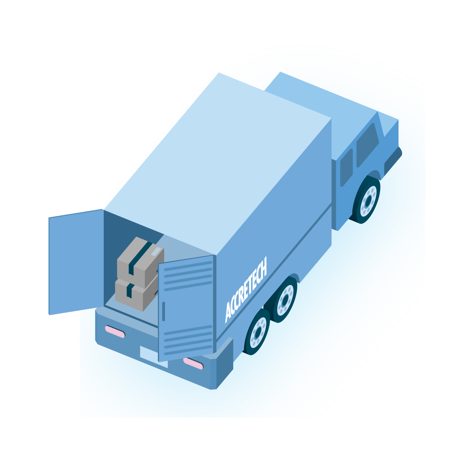
Diagram of the shipping process

FAQ

よくある質問

ここにテキストがはいりますこれはダミーテキストですここにテキストがはいりますこれはダミーテキストですここにテキストがはいりますこれはダミーテキストです。

ここにテキストがはいりますこれはダミーテキストです

ここにテキストがはいりますこれはダミーテキストですここにテキストがはいりますこれはダミーテキストですここにテキストがはいりますこれはダミーテキストです。

ここにテキストがはいりますこれはダミーテキストです

ここにテキストがはいりますこれはダミーテキストですここにテキストがはいりますこれはダミーテキストですここにテキストがはいりますこれはダミーテキストです。

ここにテキストがはいりますこれはダミーテキストです

ここにテキストがはいりますこれはダミーテキストですここにテキストがはいりますこれはダミーテキストですここにテキストがはいりますこれはダミーテキストです。

ここにテキストがはいりますこれはダミーテキストです

ここにテキストがはいりますこれはダミーテキストですここにテキストがはいりますこれはダミーテキストですここにテキストがはいりますこれはダミーテキストです。

ここにテキストがはいりますこれはダミーテキストです

ここにテキストがはいりますこれはダミーテキストですここにテキストがはいりますこれはダミーテキストですここにテキストがはいりますこれはダミーテキストです。