SEMICON Japan 2025

Date
2025-12-17(Wed) to 2025-12-19(Fri)
Host Area
Japan
Venue
Tokyo Big Sight
Official website
Booth No.
East Hall 5 E5446
Our booth overview
Tokyo Seimitsu is actively pursuing technological development in both the semiconductor manufacturing equipment and precision measuring instrument businesses, and we will be making proposals that will contribute to improving productivity in your manufacturing processes.This year, under the theme “Gaging the Future with Metrology, Creating the Future with Semiconductors,” we will introduce semiconductor manufacturing equipment that supports PLP (Panel Level Package) and solution examples focused on semiconductor substrates (wafer measurement) using our precision measuring instrument.
We look forward to seeing you at our booth.
Exhibit machines
|
New-Generation Ultra-High-Performance Probing Machine for large probe card and test head Supports PLP(Panel Level Package) |
Fully automatic blade dicing machine that supports large packages |
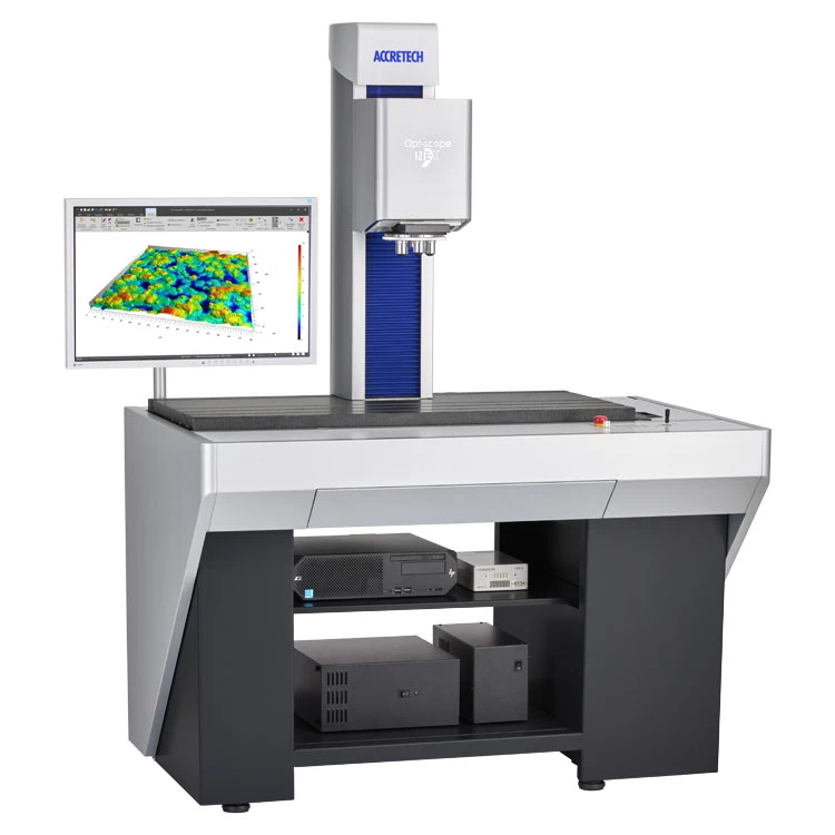
Precision Measuring Instrument |
|
 |
 |
 |
|
| Products |
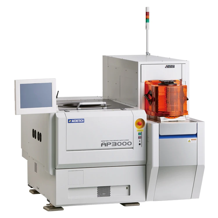
AP3000eW |
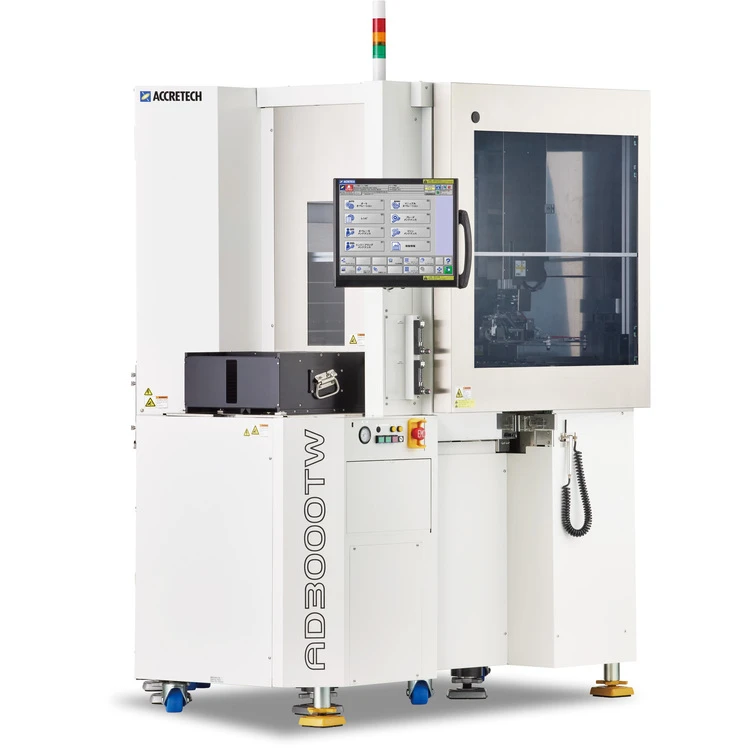
AD3000TW |
Precision Measuring Instrument |
| Overview |
AP3000W/AP3000eW is a new-generation ultra-high- performance probing machine which achieves high precision, high throughput (index move, wafer handling, and wafer alignment), low vibration and low noise. |
The dedicated design is specialized for large package substrate dicing, starting with the fan-out WLP. |
As the only semiconductor manufacturing equipment manufacturer with metrology business, we will be presenting precision measuring instruments that are ideal for measurement of parts to semiconductor manufacturing equipment. |
| Products page |