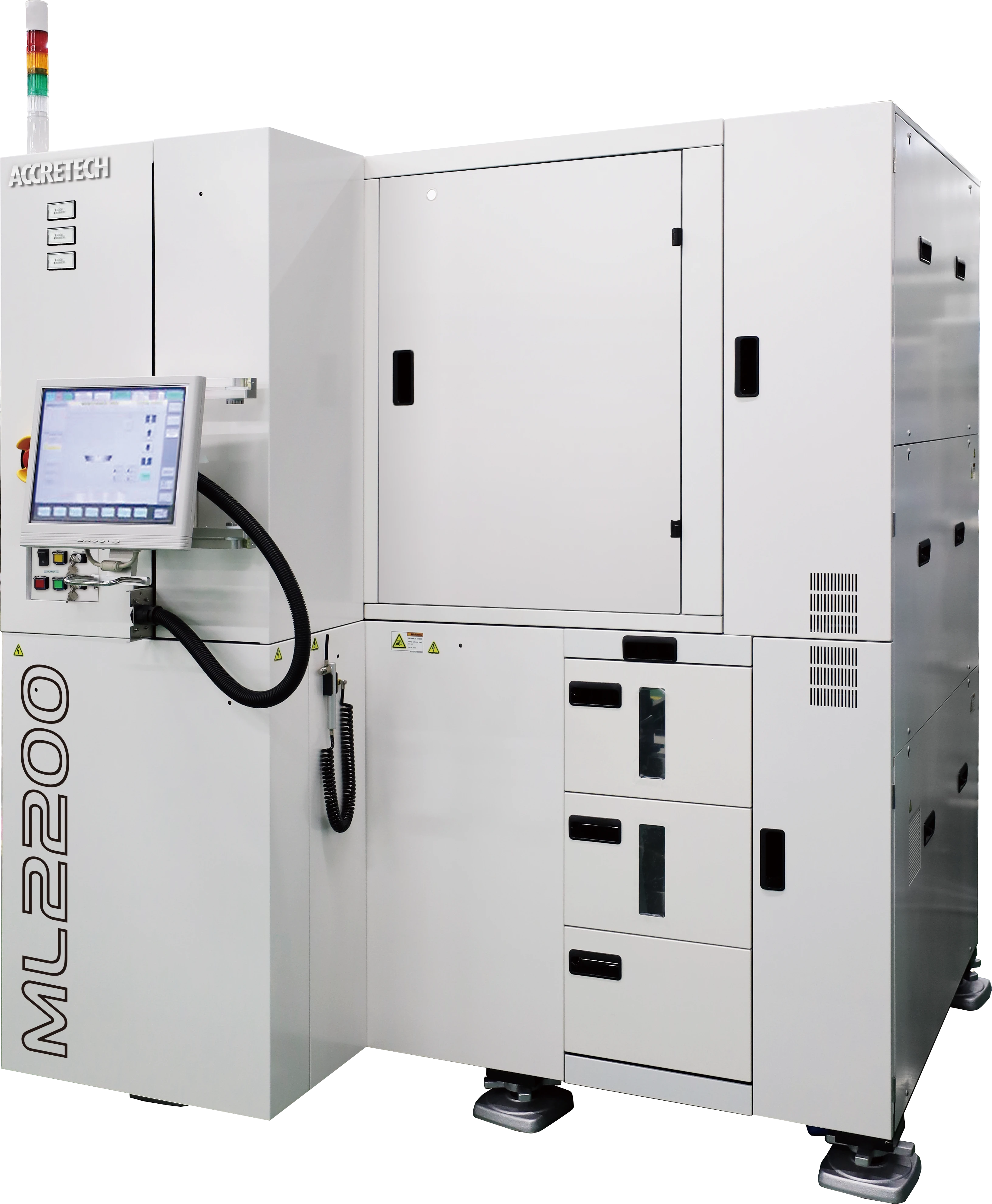
ML2200
Features
Contactless dicing is possible without damaging the silicon wafer surface
A completely dry process is supported which is ideal for processing such as for a MEMS device which does not tolerate a processing load and water.
A broad range of thicknesses can be supported, from thin items to thick items, by adjusting the number of processing scans depending on the silicon wafer thickness.
A significant reduction in cost through the increased yield
Narrowing down the dicing scribe width contributes to a significant increase in yield and a reduction in cost.
In the case of a small chip device with a wafer size of Φ 200 mm and a chip size of 1.0 mm, the chip yield is increased by 20% or more by changing the design of the dicing scribe from 90 μm to 20 μm.
Enhanced productivity (throughput)
A high-rigidity platform is used. High-speed dicing of 800 mm/sec or greater is available through the high-output laser combination.
Plenty of optional settings
A broad range of optional features are lined up related to processing quality and productivity, such as a device internal clean (class 100) specification, and a wafer thickness measurement feature.
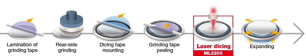
LAG(Laser After Grinding)Process
Features
The completely dry process is ideal for dicing such as for a MEMS device that abhors water.
Cost reduction is possible through the increased yield due to narrowing down the dicing street width.
Specifications
| Maximum wafer size | Φ200 mm | |||||||||||||||||||||||||||||
| Handling method | Frame handling | |||||||||||||||||||||||||||||
| X axis | Send speed entry range |
0.1 to 1,100 mm/sec |
||||||||||||||||||||||||||||
| Y axis | Resolution | 0.0002 mm | ||||||||||||||||||||||||||||
| Positioning precision | Within 0.002 mm/210 mm | |||||||||||||||||||||||||||||
| Specifications | Dimensions (W x D x H) | 1,640 mm×1,340 mm×1,800 mm | ||||||||||||||||||||||||||||
| Weight | 2,000 kg | |||||||||||||||||||||||||||||
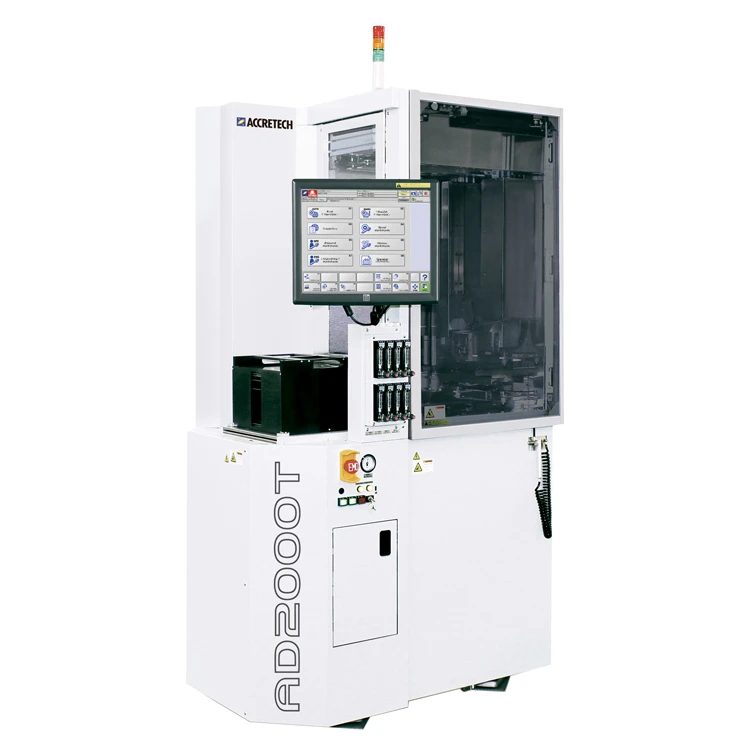
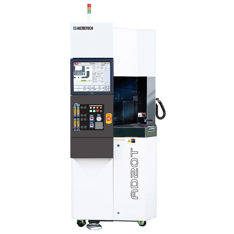
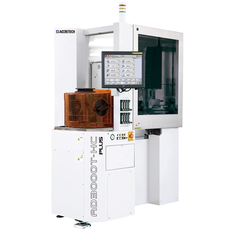
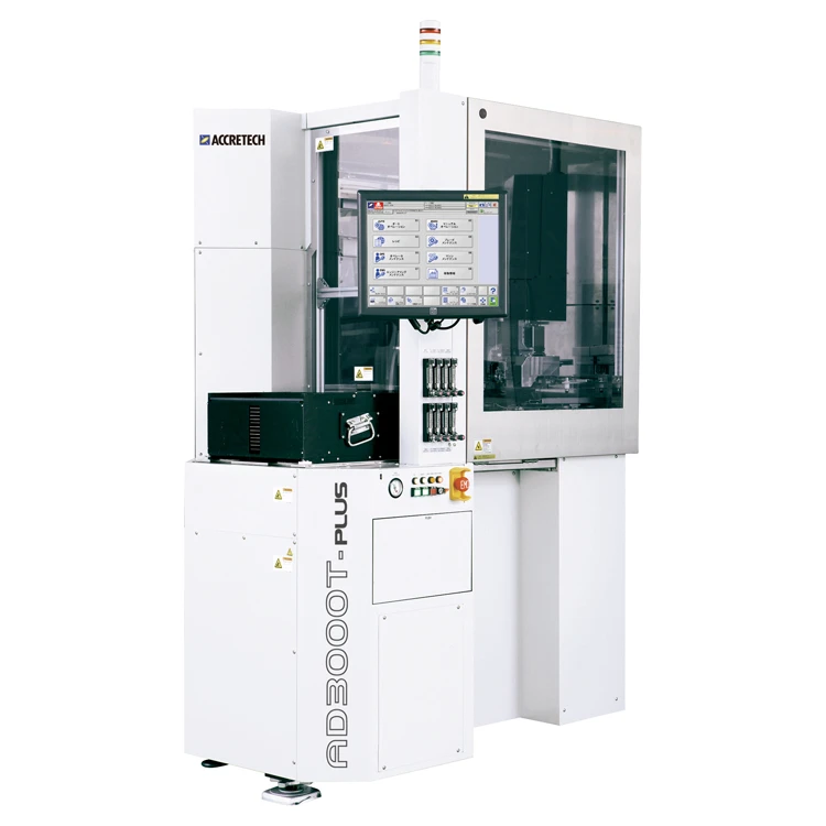
Related Products